
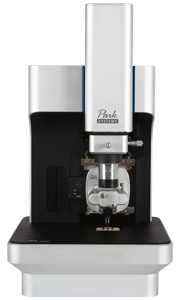
Accurate AFM Solutions for General Research
Tall Sample 1.5 µm step height
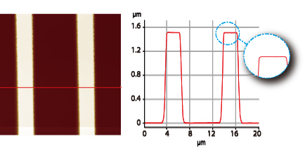
- Scan Mode: Non-contact mode, Topography from Z position sensor
Flat Sample Atomic steps of sapphire wafer
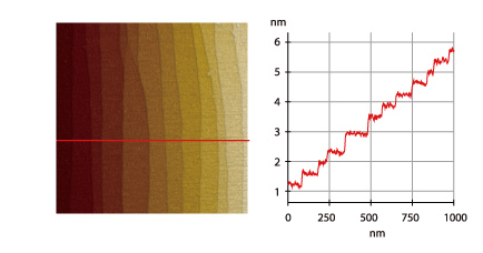
- 0.3 nm step height, Scan Mode: Non-contact mode, Topography from Z position sensor
Hard Sample Tungsten film
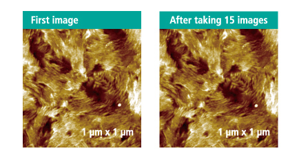
- Scan Mode: Non-contact mode, Topography from Z position sensor
Soft Sample Collagen fibril
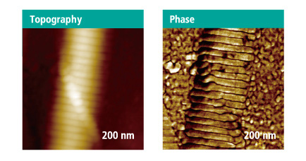
- Scan Mode: Non-contact mode, Topography from Z position sensor
Accurate AFM Measurement with Low Noise Z Detector
Low Noise Z Detector of Park nx10 AFM
- Key technological advance and design feature of NX platform
- Noise level is the lowest in the industry, unmatched by any other
- Used as the default topography signal
The Z detector is the key technological advance of the new NX-series AFM. It is a new type of strain gauge sensor, innovated by Park. At 0.2 Angstrom, it is the best Z-detector noise in the industry. The noise level is low enough for Z-detector to be used as the default topography signal. If we compare the new NX-series AFM with the previous generation of our AFM model, XE, one can tell the difference. If the Z-detector noise is too high, one cannot clearly observe the atomic steps on the sapphire wafer. The height signal from the Z detector of the Park NX AFM has a noise level, identical to that of the Z-voltage-based topography.
Park NX Series
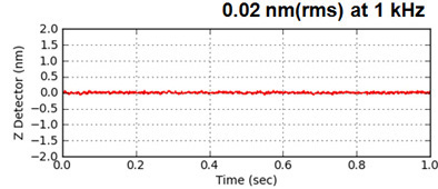 The noise level of the Z position detectors of the Park NX
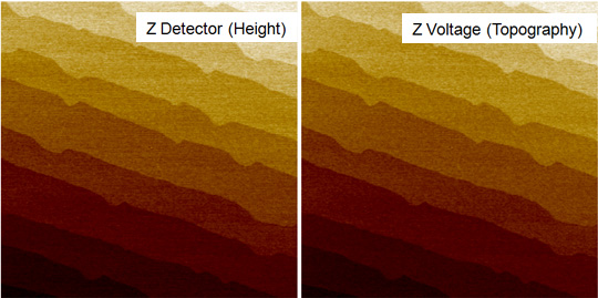 The topography images of a sapphire wafer obtained from nx10
Park XE Series
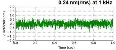 The noise level of the Z position detectors of the Park XE
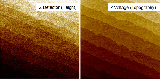 The topography images of a sapphire wafer obtained from XE-100
Accurate AFM Scan by True Non-Contact™ Mode
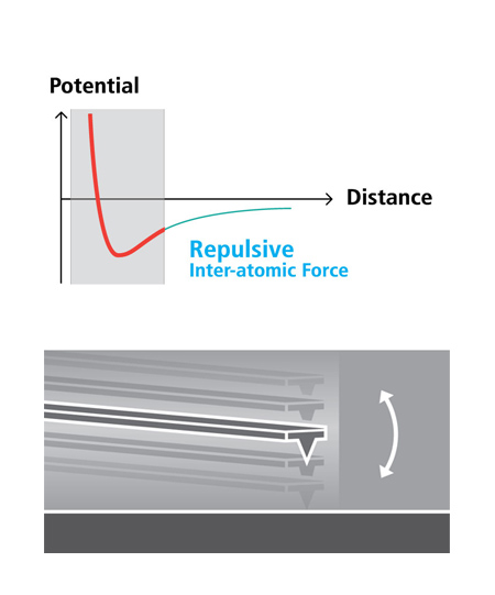
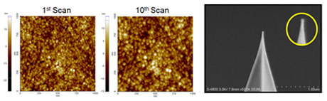
True Non-Contact™ Mode
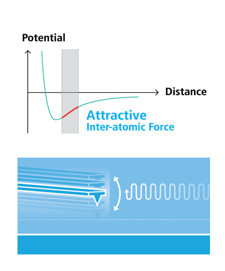
- Less tip wear = Prolonged high-resolution scan
- Non-destructive tip-sample interaction = Minimized sample modification
- Immunity from parameter-dependent results
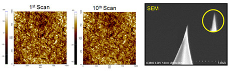
Tapping Imaging
- Quick tip wear = Blurred low-resolution scan
- Destructive tip-sample interaction = Sample damage and modification
- Highly parameter-dependent
The Best User Convenience by Design
Easy Tip and Sample Exchange
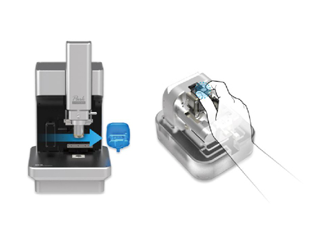
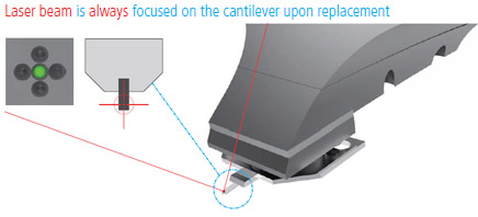
The unique head design allows easy side access allowing you to easily snap new tips and samples into place by hand. The cantilever is ready for scanning without the need for any tricky laser beam alignment by using pre-aligned cantilevers mounted onto the cantilever tip holder.
Lightning Fast Automatic Tip Approach
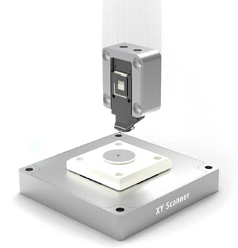
Our automatic tip-to-sample approach requires no user intervention and engages in just 10 seconds after loading the cantilever. By monitoring the cantilever response to the approaching surface, Park NX10 can initiate an automatic fast tip to sample approach within 10 seconds of cantilever loading. Fast feedback by the high-speed Z scanner and low noise signal processing by the NX electronics controller enable quick engagement to the sample surface without any user intervention. It just works, minimal user involvement required.
Easy, Intuitive Laser Beam Alignment
With our advanced pre-aligned cantilever holder, the laser beam is focused on the cantilever upon placement. Furthermore, the natural on-axis top-down view, the only one in the industry, allows you to easily find the laser spot. Since the laser beam falls vertically on the cantilever, you can intuitively move the laser spot along the X- and Y-axis by rotating its two positioning knobs. As a result, you can easily find the laser and position it on PSPD using our beam alignment user interface. From there, all you will need is a minor adjustment to maximize the signal to start acquiring the data.
Innovative features for innovative work
Park SmartScan Auto Mode
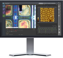
SmartScan Auto performs all the necessary operations for imaging and intelligently decides on the optimum image quality and scan speed, all autonomously. SmartScan Auto is made possible by Park’s proprietary enabling technologies. That saves you time, money, and makes for a better end result.
Park Crosstalk Elimination Technology
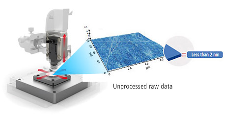
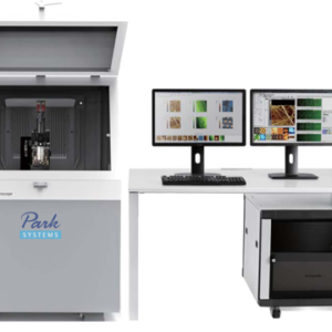
Park NX10 produces data you can trust, replicate, and publish at the highest nano resolution. It features the world’s only true non-contact AFM that prolongs tip life while preserving your sample, and flexure-based independent XY and Z scanner for unparalleled accuracy and resolution.
Park Advanced AFM Modes
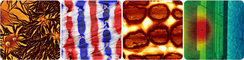
Park AFMs features a comprehensive range of scanning modes so you can collect a wide array of data types accurately and efficiently. From the world’s only true non-contact mode that preserves tip sharpness and sample integrity to advanced Magnetic Force Microscopy, Park offers the most innovative, accurate modes in the AFM industry.
Park NX10 SICM Module
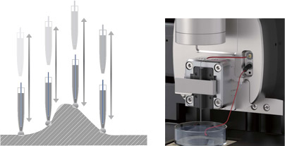
Park NX10 SICM Module provides nanoscale imaging for a wide range of applications, Cell Biology, Analytical Chemistry, Electrophysiology, Neuroscience.
Z Scanner
XY Scanner
Single module flexure XY-scanner with closed-loop control 50 µm × 50 µm (optional 10 µm × 10 µm or 100 µm × 100 µm) Resolution : 0.05 nm Position detector noise : < 0.25 nm (bandwidth: 1 kHz) Out-of-plane motion : < 2 nm (over 40 µm scan)
Stage
Z stage range: 25 mm Focus travel range: 15 mm XY stage travel range: 20 mm x 20 mm Sample size: Open space up to 100 mm x 100 mm, thickness up to 20 mm Sample weight : < 500 g
Vision
10x (0.21NA) ultra-long working distance lens (1µm resolution) 20x (0.42 NA) high-resolution, long working distance lens (0.6 µm resolution) Direct on-axis vision of sample surface and cantilever Field-of-view: 480 × 360 µm (with 10× objective lens) CCD : 1 Mpixel, 5 Mpixel (optional)
Software
SmartScan™
Dedicated system control and data acquisition software Adjusting feedback parameters in real time Script-level control through external programs (optional)
XEI
AFM data analysis software
Electronics
Signal processing
ADC : 18 channels 4 high-speed ADC channels 24-bit ADCs for X, Y, and Z scanner position sensor DAC : 17 channels 2 high-speed DAC channels 20-bit DACs for X, Y, and Z scanner positioning Maximum data size : 4096 x 4096 pixels
Integrated functions
3 channels of flexible digital lock-in amplifier Spring constant calibration (Thermal method, optional) Digital Q control
External signal access
20 embedded signal input/output ports 5 TTL outputs: EOF, EOL, EOP, Modulation, and AC bias
AFM Modes (*Optionally available)
Standard Imaging
True Non-Contact AFM PinPoint™ AFM Basic Contact AFM Lateral Force Microscopy (LFM) Phase Imaging Intermittent (tapping) AFM
Force Measurement*
Force Distance (FD) Spectroscopy Force Volume Imaging
Dielectric/Piezoelectric Properties*
Electric Force Microscopy (EFM) Dynamic Contact EFM (EFM-DC) Piezoelectric Force Microscopy (PFM) PFM with High Voltage
Mechanical Properties*
Force Modulation Microscopy (FMM) Nanoindentation Nanolithography Nanolithography with High Voltage Nanomanipulation Piezoelectric Force Microscopy (PFM)
Magnetic Properties*
Magnetic Force Microscopy (MFM) Tunable MFM
Electrical Properties*
Conductive AFM IV Spectroscopy Kelvin Probe Force Microscopy (KPFM) Scanning Capacitance Microscopy (SCM) Scanning Spreading-Resistance Microscopy (SSRM) Scanning Tunneling Microscopy (STM) Scanning Tunneling Spectroscopy (STS) Time-Resolved Photo Current Mapping (PCM)
Chemical Properties*
Chemical Force Microscopy with Functionalized Tip Electrochemical Microscopy (EC-AFM)
AFM Options
Temperature Control
Heating & Cooling Stage (-25ºC~180 ºC) 250 ºC Heating Stage 600 ºC Heating Stage
Liquid Cells
Universal Liquid Cell Electrochemistry Cell Open Liquid Cell
Liquid Probehand
Designed for imaging in a general liquid environment Resistant to most buffer solutions including acid Contact and Non-contact AFM imaging in liquid
Clip-type Chip Carrier
Can be used with an unmounted cantilever Tip bias function available for Conductive AFM and EFM Tip bias range : -10 V ~ 10 V
Magnetic Field Generator
Applies external magnetic field parallel to sample surface Tunable magnetic field Range : -300 ~ 300 gauss Composed of pure iron core & two solenoid coils
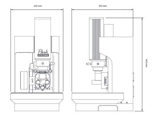
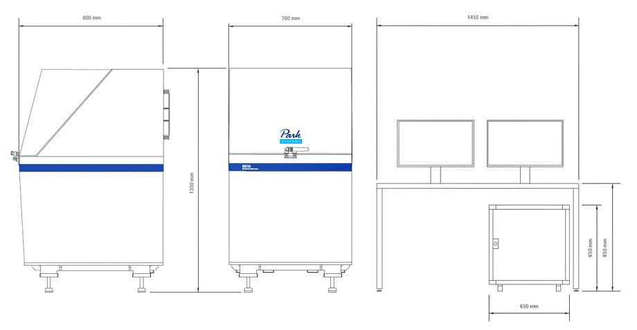
Dimensions in mm
Reviews
There are no reviews yet.